1 Purpose
The purpose of this document is to give an understanding of NAND failure modes and the measures that Yaffs takes to mitigate against these.
This document is intended to be easy reading, but some very light-weight physics is required to understand the way NAND works.
2 The NAND Cell
This section explains the internal construction of a NAND device which helps to explain the way that it fails. Each NAND cell consists of a floating gate field effect transistor, described below.
2.1 Floating Gate Field Effect Transistor
A FET is the fundamental switching element used in almost all digital electronics. A FET is a a semiconductor element that conducts when a charge is applied to the gate.
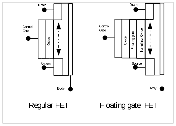
A FET is a type of semiconductor device with a semiconducting region between the the source and drain connections, an insulating oxide and a gate region. The oxide prevents current from flowing from the gate to the oxide, but applying a voltage to the gate injects charge into the gate, creating an electric field which influences the conductive properties of the semiconductor region.
In a regular FET, a conductive channel is formed between the source and drain when a suitable control voltage is applied to the gate. The current passed by the channel is dependent on the voltage (ie. the strength of the gate field). For now we will ignore analogue levels and just consider binary levels where the gate is either conducting or not. This effectively makes a switch that is controlled by the control gate.
The floating gate FET is just like a regular FET except that it has an extra floating gate. This floating gate is able to trap charge between the two insulating layers. The trapped charge modifies the local electric field and thus modifies the effect of the control gate. If the floating gate has extra electrons (negative charge) then the control gate must be raised to a higher voltage to make the FET conduct.
So a regular FET is conductive (on) when the control gate is high and is non-conductive (off) when the control gate is low. A floating gate FET, however, is only non-conductive (off) when the floating gate is charged and the gate is low. This gives us an output that is dependent on the floating gate and a way to read it (the gate).
|
Floating gate charge |
Control gate |
Source/drain channel |
|
Neutral(unprogrammed) |
High |
On (1) |
|
Neutral(unprogrammed) |
Low |
On (1) |
|
Charged(programmed) |
High |
On (1) |
|
Charged(programmed) |
Low |
Off (0) |
The tunneling oxide is insulating at low voltages but allows quantum tunneling (Fowler-Nordheim tunneling) at higher voltages. This FN-tunneling provides a mechanism to inject or remove charge from the floating gate by applying high voltages to the control gate or the body.
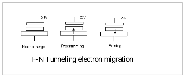
By applying a high positive voltage to the control gate, electrons are drawn into the floating gate, resulting in a programmed gate. Erasing is accomplished by the reverse operation which draws electrons out of the gate.
So a floating gate FET is effectively a readable, programmable switch. In other words: memory!
2.2 NAND array layout
NAND flash gets its name from the way that the cells are arranged. NAND cells are arranged in chains called strings, typically 1 string per bit-position in the page n(for SLC). The length of the chain is the same as the number of pages per block. This arrangement uses far less silicon area than the NOR flash arrangement which reduces NAND cost and increases density. It does however also introduce some operational and reliability problems.
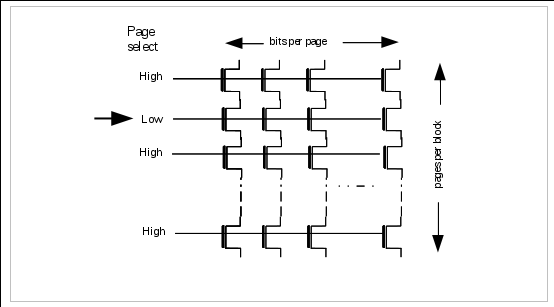
NAND is read by biasing the unselected pages with a high bias voltage and the selected pages with the low bias voltage. This means that the unselected cells are always on and the selected cells will be on or off according to the state of the floating gate.
This means we have a matrix where:
-
All unselected cells are on.
-
Selected unprogrammed cells are on
-
Selected programmed cells are off.
Since only one cell in a string is selected at a time, the whole string is on if the selected cell is unprogrammed and is off if the selected cell is programmed. Thus, even though the cells in a string are all in series we can still access them individually.
Well, that's how it would work in a perfect world anyway!
The string and block arrangement means that it takes quite a while ( typically a few µsec) for the voltage of the string to stabilize after the selection has been made. This stabilization time is the cause of the “access time” delay when accessing NAND flash.
3 Fault Modes
Sit back for a moment and consider everything that must come together for the NAND flash to work and all the ways things can go wrong:
-
Of course there can be fabrication faults where defects cause short circuits and open circuits within the chip. These types of fault apply to all chips type, not just flash.
-
Each cell has two oxide layers trapping the floating gate charge, one of which is semi-permeable to support tunneling. If either of these layers is too thick, the gate will be unresponsive. If they are too thin then the gate will tunnel too easily or will leak. If there are impurities in the oxide then the layers may become resistive and “leak”, thus causing the charge to change and possibly causing the state to change.
-
The floating gate state can change by either gaining or losing charge. If charge is lost, then a programmed cell may become unprogrammed (a 0 changes to a 1). If charge is gained, then an unprogrammed cell can become programmed.
-
In very extreme cases, a programmed cell can gain further negative charge and become over-programmed. This means that even if the high read bias voltage is applied to the control gate the FET does not become conductive. In this state, a cell will read as programmed (0) even if it is not selected. This means that the whole string will always read zero irrespective of which page is selected. This fault mode will persist until the cell is erased.
-
These devices are made very cheaply. Flash parts with tens of billions of NAND cells cost only a few dollars. There is little money to spend on individual part testing.
Extending the previous state/selection table with the over-programmed fault state, we now have:
|
Floating gate charge |
Control gate |
Source/drain channel |
|
Neutral(unprogrammed) |
High |
On (1) |
|
Neutral(unprogrammed) |
Low |
On (1) |
|
Charged(programmed) |
High |
On (1) |
|
Charged(programmed) |
Low |
Off(0) |
|
Over-charged(over-programmed) |
High |
Off(0) |
|
Over-charged(over-programmed) |
Low |
Off(0) |
4 Fault Mechanisms
This section explains some of the common NAND flash failure modes.
4.1 General chip fault
A NAND is a chip built with normal fabrication techniques and is thus prone to fail just like any other chip. Some of these faults can be isolated by marking faulty blocks. In some cases (eg. Damaged inter-block logic) the whole chip is discarded.
Yaffs does not use the bad blocks, so they have no negative impact on the performance of the file system 9apart from a small reduction in the amount of storage available).
4.2 Oxide degradation
Every programming/erasure cycle causes some degradation of the oxide layers. Over many cycles this has a tendency to degrade the properties of the oxide layer. Excessive degradation can cause the cell to fail to erase or program, but more commonly just makes the other fault modes more prevalent.
The primary mechanism of oxide degradation is that charge becomes permanently trapped within the oxide layer in a way that it is not cleared by programming and erasure. The resulting field disrupts both the FET's conductive channel and the effectiveness of the F-N tunneling.
As a result of this field disruption, two things happen:
-
The FN tunneling is disrupted which means that the programming and erasure take longer to complete. Eventually programming and erasure might fail (see Program/erase failure below).
-
The programming and erasure is far more marginal meaning that less leakage is required to corrupt a bit value (see Charge leakage below).
This degradation is permanent and incremental and is not cleared by erasure. This degradation is the cause of the endurance term in the NAND specification. Typical NAND flash endurance is 10,000 (MLC) to 100,000(SLC) program/erasure cycles.
Endurance issues are largely minimized by wear leveling and write-path caching.
Blocks that become too unreliable are retired from use.
4.3 Program/erase failure
Programming and erase operations are controlled by a built-in state machine that applies the programming/erasure voltages for a while then check whether the operation has succeeded. This is typically performed by an iterative algorithm that will time out if too many cycles are required.
A failure is signaled in the chip status register when the built-in programming/erasure mechanisms fail to accomplish the programming or erasure within the maximum program/erasure time.
It is important to realize that a programming failure is only checked on bits being set to a zero. If one bits are inadvertently set to zero then these are not raised as programming errors but are considered to be program disturb errors.
Program/erase errors are generally the result of excessive oxide degradation.
Yaffs handles programming/erasure errors as unrecoverable “hard errors”. If these are encountered then useful data is copied off the block and the whole block is permanently retired by marking the block as a bad block.
These are the only failures that the NAND devices will actually identify. All other failures need to be detected in software.
4.4 Charge leakage
The oxide isolating the floating gate is not a perfect insulator and charge can escape very slowly, particularly at temperature extremes and when the oxide had been degraded by extensive use. High radiation environments can also make this worse.
An effective way to handle charge leakage is to use ECC to detect and correct errors. Blocks with errors are rewritten on a fresh block allowing the data to be recreated before unrecoverable errors occur.
4.5 Program disturb
Program disturb happens when a bit is unintentionally programmed (1 to 0) during a programming operation. The affected bit can be in the same page or elsewhere in the block.
Program disturb is caused by bias conditions in the flash block during programming. Even though full programming voltage is only applied to the cells being programmed, the other cells are also subject to lesser voltages and minor tunneling can occur. This effect is far less than regular programming but is more than read disturb. However, since a page is only programmed once before the block is erased, there is no multiplier effect as there is in read disturb.
This condition is made worse by random programming in the block and by applying multiple partial writes to the pages.
Yaffs1 only writes pages in a block in sequential order and writes pages only once, except for writing deletion markers.
Yaffs2 does not write deletion markers and thus only programs pages sequentially and only once.
Thus, Yaffs2 is far less likely to cause write disturb. Yaffs1 should only be used with devices that are tolerant of partial page programming.
Program disturb within the same page can be corrected by verifying the page after programming.
ECC provides a mechanism to correct infrequent program disturb errors.
4.6 Read disturb
Whenever a page is read, the other pages in the block are biased at a read-inhibit voltage to turn them on. While this voltage is not as high as the programming voltage, some very slight F-N tunneling can occur. With sufficient leakage the cell state may change, or the cell may become over-programmed. This effect is known as read disturb.
Read disturb only impacts the pages in the block that are not being read. This makes it difficult to detect in some systems. For example, consider a block where only the first page is read repeatedly. Other pages in the block may be incurring read disturb but these are happening without the effect being noticed by software. By the time the pages are eventually read, the read disturb may have caused more bit errors than the ECC is able to fix.
Thankfully the problem is seldom that bad. Read disturb is very gradual. Under worst case conditions read disturb effects are expected to happen only after approximately 1 million page reads on the block for SLC flash or 100,000 page reads on the block for most MLC flash (or in other words, 10 times the endurance number).
Be warned though that as process sizes shrink, read disturb is getting more problematic. Some flash parts are prone to read disturb after 20,000 page reads.
The read disturb effect for a single read is far less than the write disturb effect for a single write. However, each page is only written once per block erase cycle but may be read many times. Therefore the cumulated effect of many read disturbs can cause problems.
Read disturb effects are cleared by erasing the block.
Various mechanisms are being implemented to correct read disturb in Yaffs, though these have not yet been implemented.
The first mechanism is to count the number of page reads on each block. When a certain threshold is reached (say 50,000 reads for an MLC part), the block is rewritten and the count is zeroed.
The second mechanism is to periodically read pages in the block. eg. Every 256 times a block has a page read we read an additional page to check for read disturb. If read disturb has happened then copy onto a fresh page.
In addition, ECC does provide some benefit, but is insufficient on its own.
5 Decoding NAND reliability statistics
Many variables contribute to NAND reliability. These variables are inter-related in complex ways which mean that is is very difficult to try to isolate the variables from each other to fully characterize them. The major variables are:
|
Temperature |
Temperature impacts the performance of the materials and thus impacts the movement of charge within the NAND cells. |
|
Storage time |
This is related to the cell leakage. The leakage integrates over time so the longer the cells are stored, the more it changes. |
|
Manufacturing variance |
|
|
Operating voltage |
|
|
Erasure/programming cycles |
|
|
Read cycles |
|
6 MLC vs SLC
Both multi-level cell (MLC) and single-level cell (SLC) NAND cells work by trapping charge in the floating gate. By trapping different amounts of charge in the gate it is possible to modify the conductance of the string. MLC store two bits in once cell by using three threshold voltages to distinguish different cell charge levels1.
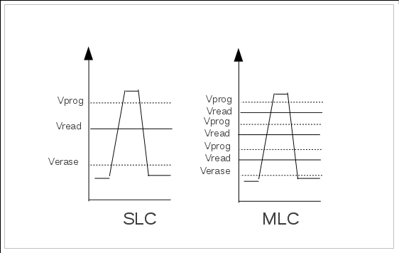
In the case of SLC, the cells are erased by the erasure state machine until the cell voltage is below V erase. Programming is accomplished by programming until the voltage exceeds Vprog. On reading, the voltage is compared with Vread.
MLC programming is accomplished in the same way, except that there are multiple Vprogs and Vreads. This means that there is far less margin for error and cell disturbance is far more likely to cause state changes.
For this reason, MLC is less reliable, has lower endurance numbers and lower read-disturb numbers. MLC thus requires far better ECC strategies to ensure reliable storage.
But MLC is cheaper!
7 Summary
In summary, NAND flash has many failure modes but these can be corrected in software to provide a reliable storage solution. Any flash storage mechanisms that do not provide sufficient coverage of different fault modes should be considered suspect.
|
|
Chip Fault |
Degradation |
P/E failure |
Leakage |
Write Disturb |
Read Disturb |
|
NAND self check |
Yes |
|
Yes |
|
|
|
|
Block retirement |
Yes |
Yes |
Yes |
|
|
|
|
Wear levelling |
|
Yes |
|
|
|
|
|
Write Verification |
|
|
|
|
Yes |
|
|
Read counting/ re-write |
|
|
|
|
|
Future |
|
Infrequent read checking |
|
|
|
Future |
Future |
Future |
|
ECC |
|
Yes |
|
Yes |
Yes |
Yes |
|
Occasional rewrite of oldest data |
|
Yes |
|
Yes |
|
Yes |
Thus all fault mechanisms are covered by at least two corrective mechanisms (read disturb correcting features are planned).
1Some MLC parts store more than 2 bits per cell, Storing n bits requires 2n levels.